STEPS TO CREATE GERBER FILE
Before generating Gerber files from Eagle, firstly you need to confirm the silkscreen is on single side or double sides, because only the top silkscreen layer (tPlace and tNames) would be generated by default in Eagle software. When your PCB has double sides silkscreen, you need to add the bottom layer as well (Dimension, bPlace and bName). If there is any milling design in your brd file, please add extra outline layer and check the”Dimension” /span> “Milling”. After following the 4 steps you will have all the necessary files needed for PCB manufacturing.
1. Generating Drill Files
To create a Gerber file in Eagle, you should run the drillcfg command first:
File –>Run ULP –> the pop-up “Drill Configuration” dialog box and click the “OK” button to generate the corresponding drill configuration file.

Open the .brd file, and then click the “File” menu to open the “CAM Processor” dialog box.

In the “CAM Processor” dialog box, select “File” -> “Open” -> “Job …” command, open the “Open CAM Job” dialog box, select the “excellentone.cam” and click “Open” button.

After loading it, click the “Process Job” command to generate the corresponding drill file:

2. Generating Gerber Files
In the “CAM Processor” dialog box, select “File” -> “Open” -> “Job …” command, open the “Open CAM Job” dialog box, select one of the “gerb274x.cam” and click “Open” After it is loaded, click the “Process Job” command to generate the corresponding Gerber file:

Please note: When it is the double layers silkscreen of your PCB, you need to add the bottom layer as well in the CAM Processor (20 Dimension,22 bPlace and 26 bNames).
Click “Add” –> Change Section to something like “Silkscreen bl”– > Change File to “%N.pls”–> Deselect all layers –> Select layers 20 Dimension, 22 bPlace and 26 bNames


If there is any milling design in your brd file, please add extra outline layer and check the “20 Dimension” and “46 Milling”.
Click “Add” –> Change Section to something like “Edge cut outline”– > Change File to “%N.gko”–> Deselect all layers –> Select layers 20 Dimension and 46 milling.

After completing the above steps, in your. brd file where the directory will generate some other documents — Gerber files ,which can be sent to the PCB manufacturers to produce.
Check the Gerber Files in Gerber View
Though you have finished generating Gerber files, you should confirm whether they are correctly functioning before folding your tools.
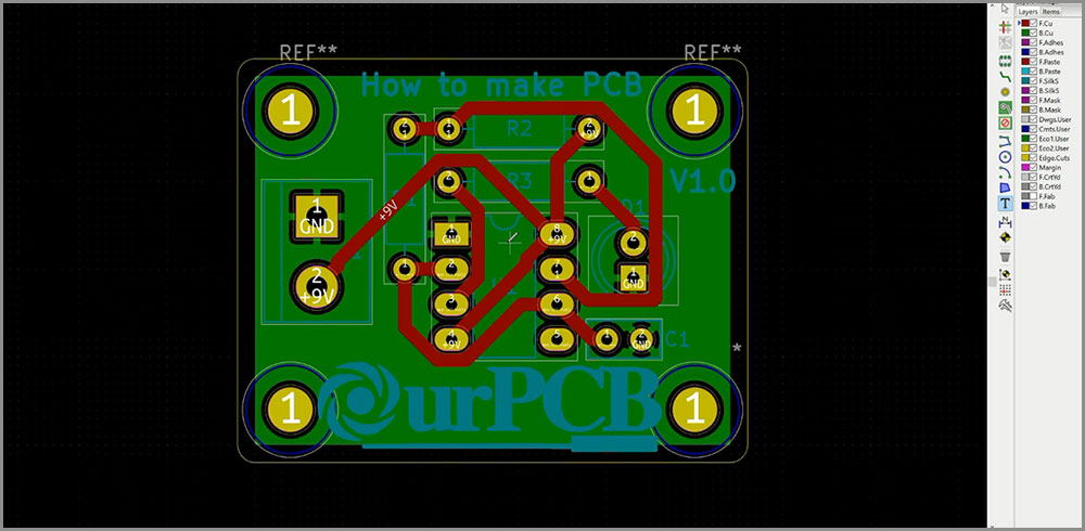
Luckily, the process of checking Gerber files is as simple as ABCD. Click the GerbView and confirm the shape and configuration of your PCB. If everything is OK, you can now send your Gerber file to your PCB manufacturer.
Your board should resemble the image below.
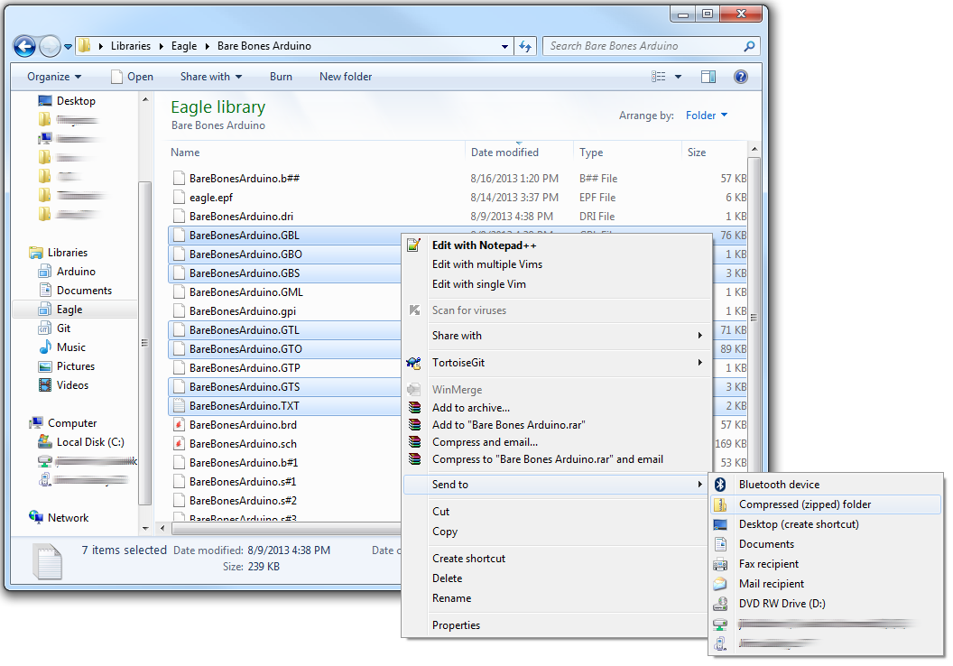
Compress your Files in a Single .zip File
Lastly, you should compress your files in one .zip file. Besides, you should fill out the document about your board features, such as size.
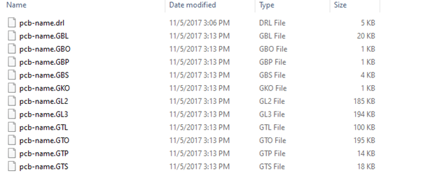
Delivering the Gerbers
The process of sending gerber files varies by fab house. Most will ask you to send them a zipped folder of select files. Which gerber files? Check with your fab house again (e.g. Advanced Circuits and OSH Park’s guidelines), but usually you want to send them GTL, GBL, GTS, GBS, GTO, GBO and the TXT files. The GTP file isn’t necessary for the PCB fabrication, but (if your design had SMD parts) it can be used to create a stencil.